












12


Solar Energy Device Laboratory
- Next-Generation Environmentally Harmonized Solar Cells
- Do all the fabrication, measurement, and analysis yourself
- Bring new waves in the photovoltaic industry
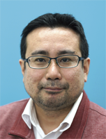
Professor / TANAKA Kunihiko, Assistant Professor / KANAI Ayaka
Professor TANAKA and Assistant Professor KANAI typically work in the student room rather than separate offices. This close proximity fosters a supportive and approachable environment. We feel comfortable consulting them at any time, whether we need technical advice on our research or guidance on personal student life.
Research Content
Our lab aims to create eco-friendly and cost-effective solar cells. We focus on:
1. Using only elements that are abundant on Earth.(Low cost)
2. Avoiding toxic materials.(Low environmental impact)
3. Fabrication via non-vacuum processes for low-cost production(even with moderate performance), or high-performance fabrication using vacuum processes.
We conduct the entire research process independently, from fabrication to characterization. We thrive in an environment that encourages autonomy, under the guidance of Professor TANAKA(Optics specialist)and Assistant Professor KANAI(Electrical properties expert).
1. Using only elements that are abundant on Earth.(Low cost)
2. Avoiding toxic materials.(Low environmental impact)
3. Fabrication via non-vacuum processes for low-cost production(even with moderate performance), or high-performance fabrication using vacuum processes.
We conduct the entire research process independently, from fabrication to characterization. We thrive in an environment that encourages autonomy, under the guidance of Professor TANAKA(Optics specialist)and Assistant Professor KANAI(Electrical properties expert).
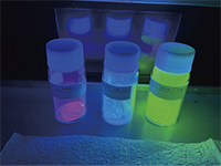
Students adjusting an equipment
A Day in the Lab
10:00 Arrive at the lab. Analyze data and write reports.
12:00 Enjoy lunch. Relax and chat with lab mates.
13:00 Progress meeting. We have in-depth discussions about our research.
15:00 Lab cleanup. Keeping our workspace clean is essential.
16:00 Experiments. Conducting tests based on the meeting discussions.
19:00 Head home for a well-deserved rest.
We don’t have mandatory core hours. You are free to manage your time and create a schedule that works best for you.
12:00 Enjoy lunch. Relax and chat with lab mates.
13:00 Progress meeting. We have in-depth discussions about our research.
15:00 Lab cleanup. Keeping our workspace clean is essential.
16:00 Experiments. Conducting tests based on the meeting discussions.
19:00 Head home for a well-deserved rest.
We don’t have mandatory core hours. You are free to manage your time and create a schedule that works best for you.
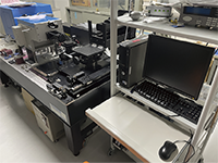
Group photo at the academic conference
Thesis Subjects
- (M)Improvement of solar cell properties for ZnO/CuBr1-xIx microstructural highly transparent solar cells by optimization of the seed layer and nanorods annealing process
- (M)Fabrication of Cu-Sn-Ge-S thin films by trio source fine channel mis CVD method
- (B)Preparation of Cu-Sn-Si-S bulk by Hot press method
The number of
PhD Graduates
1
Major employers of Graduates
- JEOL Ltd.
- Sony Semiconductor Manufacturing Corporation
- TAIYO YUDEN CO., LTD.
- Semiconductor Energy Laboratory Co., Ltd.
- NGK INSULATORS, LTD.
- Applied Materials, Inc.
- NICHIA CORPORATION
- JGC CORPORATION
- ALPS ALPINE CO., LTD.
- Hitachi High-Tech Analysis Corporation
